Safety Diode Thyristor Opamp Triac
Transistor
Target Preparing Experimentation Report Problems
Laboratory target
Making the simple transistor circuits and acquainting with input and output characteristics of a transistor in the common emitter mode of operation.
Lesson preparation
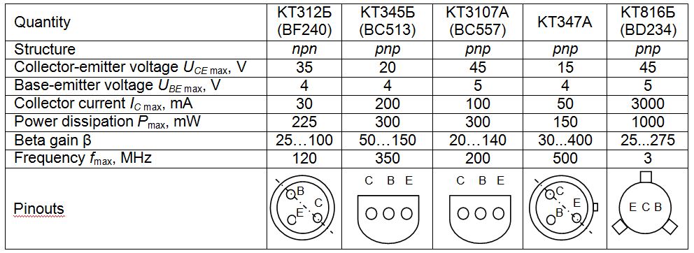
- Using the datasheet below, find the transistor data: type, permissible collector-emitter voltage UCE max, base voltage UBE max, collector current IC max, power dissipation Pmax, beta gain β, and frequency fmax. Calculate an expected base current IB max.
- Familiarise with the available power source: its voltage Us max and current Is max.
- Develop the circuit and wiring diagrams to study an input characteristic IB(UBE) at zero collector-emitter voltage UCE and output characteristics IC(UCE) at different base currents IB of a transistor in the common emitter mode of operation. Consider the pnp or npn transistor structure to select the proper supply polarity. Calculate and place a voltage divider between the power supply and the base circuit to bias and protect the base. Calculare and place another voltage divider between the power supply and the collector circuit to bias and protect the collector. Choose the potentiometers of 1 kΩ or 10 kΩ in these dividers.
- Provide the circuit link-up with:
dc voltmeter PV to measure the transistor collector-emitter voltage UCE or the base voltage UBE
dc ammeters PA1 and PA2 to measure the transistor collector current IC and base current IB
and propose the required meters: their types, measuring limits, and maximum measured values.
-
Sketch expected input and output characteristics and voltage waveforms.
Experimentation
- Choose the meters and set the required measuring ranges and sockets for wiring. Adjust the supply voltage to 10 V.
-
Find the positions of the potentiometer knobs that correspond to the maximal and minimal voltages and set the minimal voltages on their sliders.
- Assemble the desired circuit to estimate the input characteristic IB(UBE) at an open collector. Self-examine and ask an instructor to examine your circuit.
- Power on the base supply and ensure the circuit operates properly. If the fault occurs , power off the breadboard immediately, examine the circuit and eliminate errors.
- To estimate an input characteristic, increase smoothly UBE by turning the base potentiometer knob until the maximal base voltage UBE or current IB is achieved. At every step, measure the base voltage UBE and current IB, fill the measured values in the protocol, and plot the graph. Afterwards, remove the base voltage and the breadboard supply.
- Assemble the desired circuit to estimate the output characteristics IC(UCE), self-examine and ask the instructor to examine it also.
- Apply the full voltage across the collector and emitter without base signal and read the cutoff voltage UCE cutoff. Next, apply the full base voltage across the base and emitter read the saturation current IC sat .
- To plot an output characteristic, keep the constant base current IB below the IB max and increase smoothly UCE until the cutoff voltage UCE cutoff is achieved or the collector current IC reaches the saturation level IC sat . At every step, read IC, IB, UCE, write down them to the protocol, and plot the graph.
- Following the instructor’s permission, switch off the devices, take off the circuit, and introduce proper order in the workplace.
Report contents
- Wiring diagram of the experimental setup with specification of the components.
- Circuit diagram of the experimental setup.
- Calculation of voltage dividers and an expected base current.
- Tables of the observed data UBE, IB at an open collector as well as UCE, IC at given IB.
- Scaled diagrams of the experimental input and output characteristics.
- Estimation of the cutoff voltage (UBE cutoff ) and saturation current (IC sat ), load line, operating point, beta and alpha gains, as well as the differential input and output resistances at the operating point.
- Conclusions regarding estimation, comparison and explanation of the expected and obtained results.
- Signed protocol.
Optional section
-
Find an output characteristic at two other base currents and include to the report the table and the characteristic obtained, load line, operating point at observed IB, beta and alpha gains, as well as the differential input and output resistances at the operating point.
- Estimate an input characteristic at IC > 0. To this aim, keep IC < IC max and increase smoothly UBE until the permissible base current IB or cutoff voltage UBE max of the transistor is achieved. At every step, measure the base voltage UBE and current IB, fill the measured values in the protocol, and plot the graph.
- Using a signal generator and an oscilloscope, develop and employ the circuit to trace the base and collector voltage waveforms in the given point of the output characteristic.
- Design an employ an additional experiment to demonstrate the non-linear modes of the transistor operation and prove your result with simulation.
- Calculate the transistor input and output voltage drops at the operating point of the highest current gain and prove your result with simulation.
- Calculate the transistor input and output power dissipation rates at the operating point of the highest power dissipation and prove your result with simulation.
Safety Diode Thyristor Transistor Opamp Triac